


Apply Now Schedule a visit

B.Tech in Semiconductor Technology

Design, build and test the chips that power the world.
Next Cohort
July 2027
Format
4 Years, Full time

The ATLAS uGDX B.Tech Experience

The B.Tech programs in ATLAS immerses you in technology from day one - through hands-on coding, real-world projects, and industry-integrated learning that build the skills to innovate and lead in the digital world.

Multidisciplinary
Tech Education
Learn AI/ML alongside electives in design and management, applying your skills through a semester-long internship.
Master classes by industry leaders
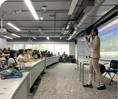
Learn directly from global technology experts, CTOs, and industry innovators.
NEP 2020
Integrated
Hundreds of hours of coding practice and training to master writing clean, scalable code.
Experiential &
Hands-on learning
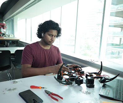
Apply classroom concepts to live projects and real-world problem solving.
Curriculum co-created with industry
Study a curriculum designed with leading CTOs to stay aligned with industry needs.
Entrepreneurship hub
Get mentorship and support from Venture Labs to build and launch your own tech startup.
Urban campus experience
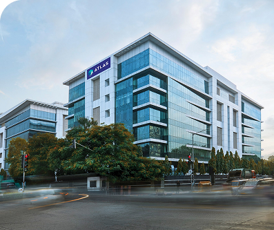
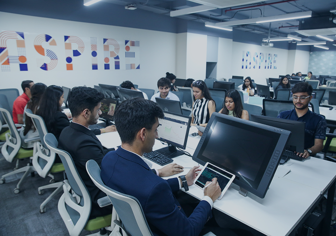
Thrive in a modern, high-tech learning environment with state-of-the-art infrastructure.
Career services
Apply classroom concepts to live projects and real-world problem solving.

Why Choose B.Tech in Semiconductor Technology at ATLAS uGDX

From Sand to Silicon

Unlike typical electronics programs, you learn the full chip lifecycle — materials, device physics, design, fabrication, packaging and testing — in one degree.
01

Hands-on Cleanroom & EDA Training

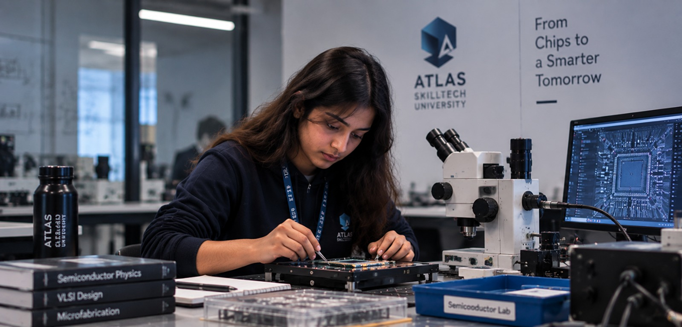
Fabricate real silicon devices across three cleanroom lab courses and take designs from code to chip layout using professional and open-source EDA tools.
02

Three Specialisation Tracks In Year 4

In Year 4, specialise in VLSI & Chip Design, Fabrication & Manufacturing, or Compound Semiconductors — each supported by dedicated labs and electives.
03

Aligned with the India Semiconductor Mission

Built around India's growing chip design, fab and packaging ecosystem, preparing you for the roles the country's semiconductor push is creating.
04

Global Exposure to Technology Policy & Sustainability

Through the ATLAS Global Week and international faculty exchange, explore the global chip supply chain, semiconductor IP law and sustainable manufacturing.
05

A Curriculum Designed for the Future

Built on the ‘Goal for Each Term’ (GET) philosophy, our curriculum ensures every semester has a clear, outcome-driven focus; continuously evolving with emerging technology trends and the learning needs of our students.

Semester 1

Building the Engineering Foundation
The first semester builds a strong base in mathematics, physics, chemistry and programming, while introducing students to how semiconductors are designed, made and used across the world.
Engineering Mathematics I
Covers calculus and linear algebra to build a strong foundation for modelling and analysis.
Engineering Physics I
Explores mechanics, waves and optics through theory and hands-on labs.
Engineering Chemistry
Studies materials and electrochemistry, the chemistry behind chip manufacturing.
Introduction to Semiconductor Engineering
Explains what semiconductors are, how chips are made and why they matter.
Programming for Engineers: Python & C
Develops coding and problem-solving skills through hands-on exercises.
Engineering Graphics & Technical Drawing
Builds skills to read and create precise technical drawings.
Communication Skills for Engineers
Builds writing, presentation and teamwork skills for technical environments.
Multidisciplinary Elective I
Broaden your worldview with a course in AI, management or biology.
Environmental Studies
Introduces sustainability and environmental responsibility in engineering.

Semester 2

Materials & Circuit Fundamentals
Students explore the materials that make chips possible and learn how electronic devices and digital circuits work, while connecting India's heritage in metallurgy to modern materials science.
Engineering Mathematics II
Covers differential equations and complex analysis used in circuits and device modelling.
Engineering Physics II
Explores electromagnetism and modern physics, the science behind electronics.
Materials Science for Semiconductors
Studies silicon and other materials and how their properties shape device performance.
Electronic Devices & Circuits
Explains diodes, transistors and circuits through theory and lab work.
Digital Logic Design
Shows how binary logic and digital circuits form the basis of every chip.
Indian Knowledge Systems I
Connects India's ancient metallurgy and materials heritage to modern semiconductor materials.
Multidisciplinary Elective II
Strengthen your multidisciplinary learning portfolio.

Semester 3

Inside the Semiconductor
Students go deep into semiconductor physics and device theory, learning how junctions and transistors work at the atomic level, and how thin films are deposited to build devices.
Semiconductor Physics & Devices I
Covers PN junctions and bipolar transistors, the building blocks of electronics.
Quantum Mechanics for Engineers
Explains the quantum behaviour of electrons that governs every semiconductor.
Solid State Physics
Studies crystal structures and energy bands in solid materials.
Electromagnetic Theory
Builds understanding of electric and magnetic fields in devices and circuits.
Thin Film Technology & Deposition Processes
Learn how ultra-thin material layers are deposited to build chips.
Electronics Lab — Devices & Characterisation
Measure and analyse the behaviour of real electronic devices.
Design Thinking & Innovation for Hardware
Apply design thinking to solve real hardware problems and build prototypes.
Multidisciplinary Elective III
Explore a course beyond your core discipline.

Semester 4

Into the Cleanroom
Students learn how transistors are manufactured and step into the cleanroom for the first time, fabricating silicon devices and learning how chips are measured and quality-controlled.
Semiconductor Physics & Devices II
Covers MOSFETs and advanced devices that power modern processors.
Semiconductor Fabrication Processes I
Learn oxidation, diffusion and ion implantation, the core steps of chip making.
Signals & Systems for Semiconductor Engineers
Understand how signals are analysed and processed in electronic systems.
Metrology & Characterisation Techniques
Learn how chip features are measured and inspected at the nanoscale.
Cleanroom Lab I — Silicon Device Fabrication
Fabricate your first silicon devices in a cleanroom environment.
Statistical Methods for Process Engineering
Apply statistics to control quality and improve manufacturing yield.
Environmental Science & Semiconductor E-Waste
Examine the environmental impact of chip making and e-waste management.
Multidisciplinary Elective IV
Round out your learning with an elective that fits your ambitions.

Semester 5

Designing & Building Chips
Students begin designing digital chips using hardware description languages while mastering advanced fabrication steps such as lithography and etching, along with analog and power devices.
VLSI Design I: Digital CMOS Design & HDL
Design digital circuits and write hardware code using Verilog.
Semiconductor Fabrication Processes II
Learn lithography, etching and polishing techniques used in modern fabs.
Analog & Mixed-Signal Circuits
Design circuits that connect the digital world to real-world signals.
Power Electronics Devices
Study power MOSFETs, IGBTs and SiC devices used in EVs and energy systems.
Cleanroom Lab II — Advanced Process Integration
Combine multiple fabrication steps into integrated process flows.
Semiconductor Reliability & Failure Analysis
Learn why chips fail and how to make them last longer.
Entrepreneurship in the Semiconductor Industry
Explore the chip value chain and how semiconductor startups are built and funded.

Semester 6

Packaging, Testing & Industry Integration
Students complete the chip lifecycle, from physical design and advanced fabrication to packaging and testing, and apply AI to manufacturing data before a summer internship in industry or research.
VLSI Design II: Physical Design, STA & DFT
Turn chip designs into layouts and verify timing and testability.
Advanced Semiconductor Fabrication
Learn ALD, CVD, PVD and epitaxy used in advanced chip nodes.
Semiconductor Packaging & Assembly Technology
Understand how chips are packaged, assembled and connected to the world.
Semiconductor Testing & ATE
Learn how chips are tested at scale using automated test equipment.
Compound Semiconductors: GaN, SiC & III-V
Explore next-generation materials for power, RF and optoelectronics.
AI & Data Analytics for Semiconductor Manufacturing
Apply AI and data analytics to improve yield and quality in fabs.
Cleanroom Lab III — Full Process Flow Fabrication
Take a device through a complete fabrication process flow.
EDA Tools & Semiconductor Data Skills
Build hands-on skills in chip design tools and fab data analysis with Python.
Indian Knowledge Systems II
Connect Indian mathematics and logic to modern digital computing.
Seminar I: Semiconductor Industry Trends & Research
Explore the latest research and trends shaping the chip industry.
Summer Internship
Gain real-world experience with a semiconductor company or research lab.

Semester 7

Choose Your Specialisation
Students choose one of three specialisation tracks and go deep into their field, supported by a research internship or lab rotation and seminars on emerging semiconductor technologies.
Common to All Tracks
Research Internship / Lab Rotation
Work on live projects in an industry, fab or research lab.
Seminar II: Emerging Semiconductor Technologies
Review cutting-edge research and the future of chip technology.
Professional Elective I
Choose an advanced elective from your track's pool.
Constitution of India
Understand India's constitutional values and framework.
Track A — VLSI & Chip Design
Advanced VLSI Physical Design & Tapeout
Take a chip design all the way to tapeout.
Functional Verification: UVM & Formal
Ensure chip designs work correctly using industry verification methods.
Analog Mixed-Signal IC Design
Design complex analog and mixed-signal integrated circuits.
Track B — Fabrication & Manufacturing
EUV Lithography & Multi-Patterning
Learn the advanced lithography behind the world's smallest transistors.
Yield Engineering & Process Integration
Maximise the number of working chips from every wafer.
Advanced Packaging: 2.5D/3D IC & FOWLP
Explore advanced packaging that stacks and connects chips.
Track C — Compound Semiconductors
GaN/SiC Device Fabrication
Fabricate wide-bandgap devices for power and RF applications.
Photonics & Optoelectronics
Study light-based devices such as LEDs, lasers and photodetectors.
Wide Bandgap Power Electronics
Design high-efficiency power systems for EVs, energy and defence.

Semester 8

Capstone & Industry Readiness
The final semester brings everything together in a major capstone project or research thesis, alongside courses on semiconductor industry management, intellectual property and entrepreneurship.
Capstone Project / Research Thesis
Apply your learning to a major end-to-end semiconductor project or research thesis. (Pinnacle Project)
Seminar III: Semiconductor Entrepreneurship & Future Technologies
Explore startups, policy and the future of the chip industry.
Semiconductor Industry Management & IP Law
Learn how chip innovations are protected, managed and commercialised.
Open Elective
Choose an elective that complements your career goals.
Comprehensive Viva Voce
Demonstrate your complete understanding of the program.
Yoga & Wellness
Build balance and well-being as you step into your career.

Program Outcomes

Design Next-Generation Chips
Design digital, analog and mixed-signal chips from code to layout using industry-standard EDA tools.
Fabricate Semiconductor Devices
Operate cleanroom processes to fabricate, measure and characterise semiconductor devices.
Package, Test & Assure Quality
Apply packaging, testing and reliability techniques to deliver chips that work and last.
Drive Smart Manufacturing
Use statistics, AI and data analytics to improve yield and quality in semiconductor fabs.
Integrate Multidisciplinary Problem Solving
Blend physics, materials, electronics and design thinking to create real-world hardware solutions.
Lead India's Semiconductor Innovation
Drive research, entrepreneurship and sustainable innovation aligned with the India Semiconductor Mission.

Ready to Build What’s Next?Let’s Get Started.

Get a glimpse - where future engineers and innovators areshaped through technology, industry, and inspiration.

Career Pathways

Explore diverse career pathways across chip design, manufacturing and emerging semiconductor technologies.

VLSI Design Engineer
Verification Engineer
Analog / Mixed-Signal IC Designer
Process Engineer
Yield Engineer
Packaging & Assembly Engineer
Test & Validation Engineer
Power Electronics Engineer

Your guide to joining B.Tech in Semiconductor Technology at ATLAS uGDX

Eligibility
    Indian Boards (ISC / CBSE / State Boards)
    Minimum 50% in Class XII
    Mathematics and Physics are mandatory

    A-Levels (UK)
    Minimum grades A/B/C in 2 subjects
    Grade B or above in Mathematics.
    Mathematics and Physics are mandatory

    International Baccalaureate (IB)
    Minimum of 24 points in 3 HL & 3 SL subjects
    Mathematics and Physics are mandatory
    More questions?
    Let our AI Assistant answer your queries

    Questions? We can read your mind

    The program covers the complete life of a chip — semiconductor materials and physics, chip design (VLSI), fabrication, packaging and testing — with hands-on training in cleanroom labs and industry-standard design tools.

    Yes. Through the India Semiconductor Mission, India is investing in chip fabs, packaging units and design companies, creating strong and growing demand for trained semiconductor engineers.

    Students who enjoy physics, mathematics and electronics, and want to build the hardware that powers phones, computers, cars and AI, will find this program a great fit.

    Students need a minimum of 50% in Class XII (ISC / CBSE / State Boards) with Mathematics and Physics, or equivalent A-Level or IB qualifications. See the eligibility section above for details.

    Admission is through the uGDX Challenge followed by a personal interview. Complete the online application form to get started.

    Core subjects include semiconductor physics and devices, materials science, VLSI design, fabrication processes, analog and mixed-signal circuits, packaging, testing, reliability and compound semiconductors.

    Students learn how AI and data analytics are used to improve manufacturing yield, detect defects and speed up chip design, through a dedicated course and hands-on projects with Python.

    Yes. The program includes three cleanroom lab courses, an electronics and device characterisation lab, and hands-on EDA tool training for chip design.

    In Year 4, students choose one of three tracks: VLSI & Chip Design, Fabrication & Manufacturing, or Compound Semiconductors.

    Yes. Students complete a summer internship in Year 3 and a research internship or lab rotation in Year 4, followed by a capstone project or research thesis.

    Graduates can work as VLSI Design Engineers, Verification Engineers, Process Engineers, Yield Engineers, Packaging Engineers, Test Engineers and Power Electronics Engineers, or start their own hardware ventures.

    Chips power almost every modern technology, from smartphones and EVs to AI and defence. As India builds its own semiconductor ecosystem, skilled engineers will be needed across design, manufacturing and packaging.

    Yes. The ATLAS career services team supports students with internships, industry connections and placement opportunities across the semiconductor and electronics ecosystem.

    The campus is located at Equinox Business Park, Bandra-Kurla Complex (BKC), Kurla West, Mumbai, with modern classrooms, labs and collaborative learning spaces.

    It is a 4-year, full-time program spread across 8 semesters.